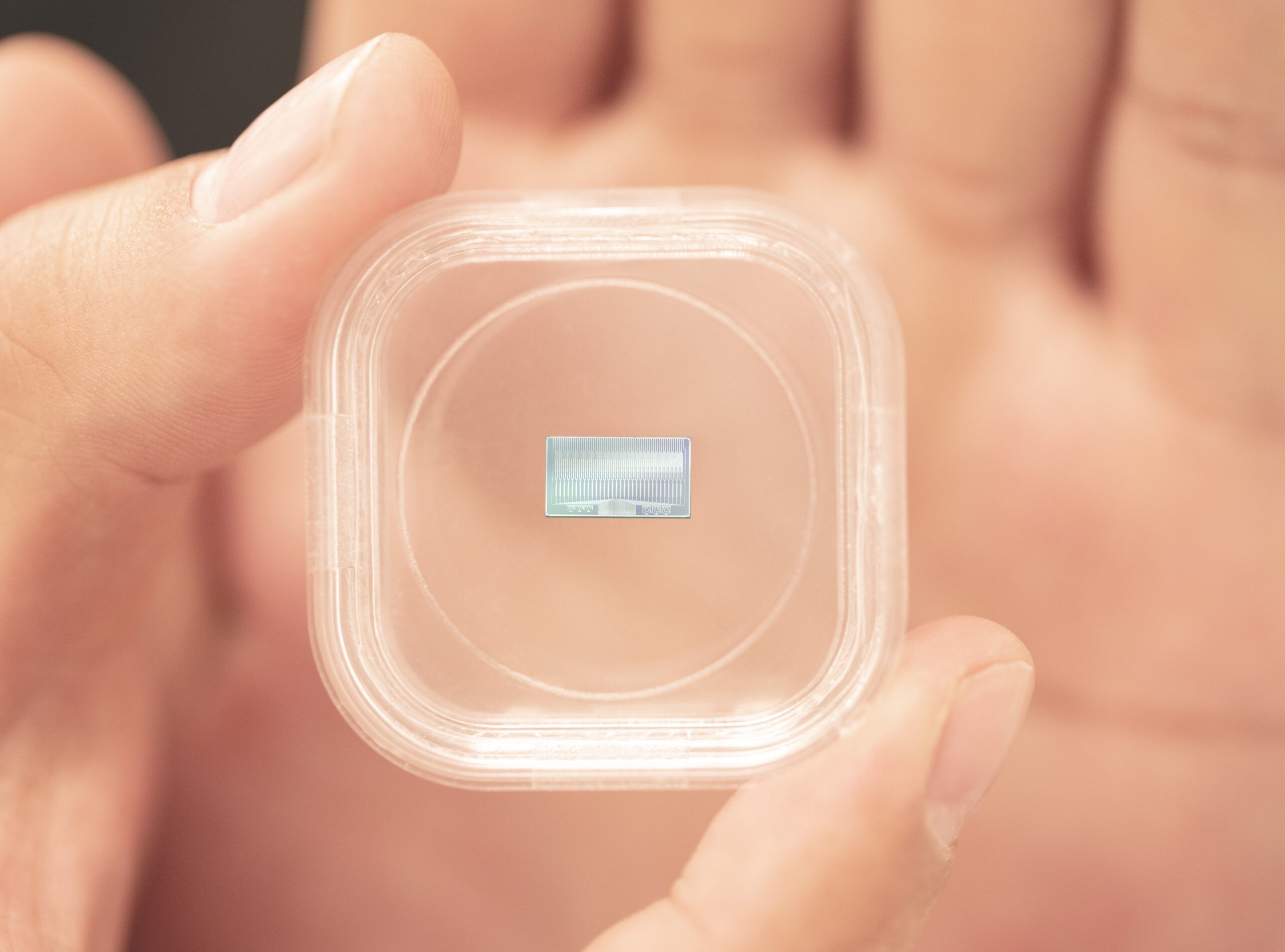
Scantinel is a world-leading FMCW LiDAR start-up company, headquartered in Ulm, Baden-Württemberg, Germany. Incubated in the global optics leader Carl Zeiss AG in 2016, Scantinel spun off as an independent company in 2019 backed by ZEISS Ventures, Scania Growth Capital and PhotonDelta. In January 2026, Scantinel became a subsidiary of MicroVision, Inc.
We are building best-in-class FMCW LiDAR technology for future mobility applications. FMCW LiDAR systems will help create unparalleled safety level in automotive, mobility, trucking, and for industrial application.
Deine Aufgaben
Design and develop wafer level packaging solutions, 2D/2.5D/3D, for advanced silicon photonics platforms
Create and optimise metallisation layouts (e.g. UBM, RDL, Solder, TSVs) to meet electrical, mechanical and manufacturing requirements.
Define and engineer package mechanical features, including die interfaces, alignment structures, stress management and assembly tolerances.
Perform thermal modelling and analysis to optimise heat dissipation, thermal resistance and package reliability across operating conditions.
Develop and execute package validation plans, including optical performance, mechanical, thermal, and reliability testing of finished hardware, analysing results and driving design improvements.
Collaborate with process, assembly and foundry partners to ensure package designs are compatible with wafer level fabrication, bonding and high-volume manufacturing processes.
Conduct package verification through simulation, design reviews and failure analysis, driving continuous improvement in performance, manufacturability and yield.
Support the integration of photonic devices by considering package impacts on optical alignment, optical coupling efficiency and overall system performance, working closely with photonic design teams.
Dein Profil
A Master or PhD in Packaging Engineering, Photonics, Mechanical Engineering, Physics or a related discipline.
Proven experience in advanced semiconductor packaging with exposure to wafer-level packaging, flip-chip, interposer, chiplet, 2D, 2.5D or 3D integration technologies.
Experience using mechanical and thermal simulation tools (e.g. ANSYS, COMSOL or equivalent) for package design and optimisation.
Strong understanding of wafer level package metallisation design
A few years of industry or advanced research experience in wafer level packaging.
Experience with photonic device packaging, optical alignment challenges or co-packaged optics is advantageous.
Hands-on experience with electro-optical device characterization at wafer, die level or package level
ZEISS Ventures has been committed to us from our inception. And in May 2021, Scania Growth Capital joined as an investor. This investment has been made because of Scantinel's technology leadership in its field and the progress of autonomous technologies in the heavy truck industry. In November 2022, PhotonDelta, a leading photonics eco-system joined as a new investor.